Chip designers do their best to use the latest cocktail of verification techniques and tools, and EDA companies continually innovate new verification tools, design flows, and pre-verified silicon IP, in a valiant effort to achieve the elusive goal of achieving chip design verification perfection.


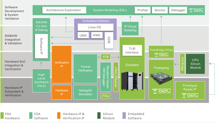
The increasing size and complexity of SOC/ASIC designs have led to an exponential increase in the complexity of validation. In order to reduce time to market, it is important to choose different verification tools in different design stages to improve efficiency and accelerate the convergence of verification.
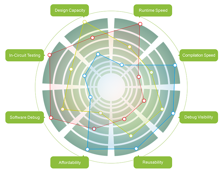
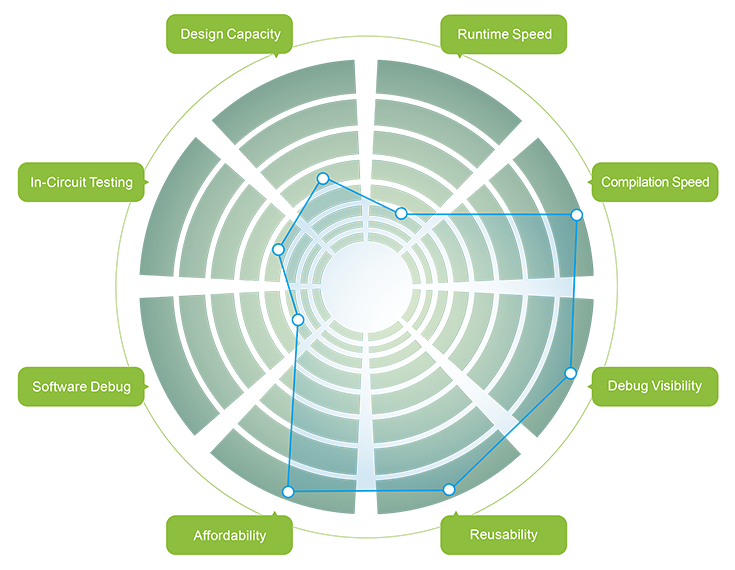
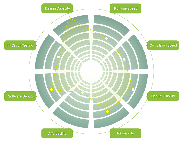
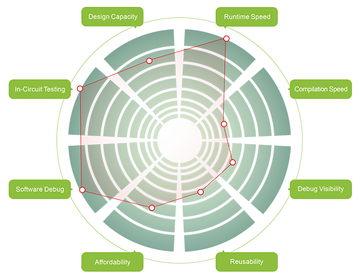
FPGA-based prototyping tools are scalable, cost-effective for almost any design, offer capable debug visibility, and are well suited to hardware-software co-verification. S2C has researched how the need for co-verification evolved with chip complexity, where FPGAs got their start in verification, and why ASIC design benefits from prototyping technology.


This site uses cookies to collect information about your browsing activities in order to provide you with more relevant content and promotional materials, and help us understand your interests and enhance the site. By continuing to browse this site you agree to the use of cookies. Visit ourcookie policy to learn more.