AIVA is a high-tech company focused on developing 3D vision AI ASIC, aiming to empower the better world with AI chip. They bring talented individuals with robust chip design, algorithm, product, and marketing skills from worldwide famous chip design companies such as AMD, Intel, Broadcom.


3D vision technology is evolving rapidly. Compared with 2D vision technology, which deals with planarinformation, 3D vision enables provide more dimension and proximity details for object recognition and measurements. Machine learning and big data computing has advanced AI for 3D vision with higher accuracy, higher speed, and lower power consumption.
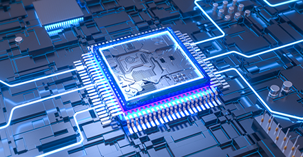
AIVA is a high-tech company focused on the research and development of 3D vision AI ASIC. Kaiying AI3101 is a new generation of 3D vision AI chip based on heterogeneous architecture. With a built-in neural network processor (NPU), 3D engine, HDR, ISP, etc., making ship has efficient and intelligent processing, analysis, and low power management ahead of the terminal field. Also, the resource reuse of AI3101 architecture enables the flexible allocation of hardware computing units, which applies to different scenarios' computing needs. It realizes the perfect integration of "core" and "computation" and provides modular solutions that are easy to be deployed, expanded, and integrated by intelligent terminal customers.
S2C has been developing FPGA prototyping platforms since 2003, and, over the years, they have catered what various/ different users want for a complete FPGA prototyping solution. Design the right product needs to come before design the product right.
 Prodigy 逻辑系统")
Using Virtex UltraScale (VU) Prodigy Logic System for SoC Prototyping
Modular and All-in-One design offering the highest flexibility and performance
Abundant prototyping tools (partition and debugging) support to speed up the prototype bring-up time
Easy reconfiguring or stacking to expand capability for several projects
Comprehensive portfolio of Prototype Ready Accessories for quickly build the prototype targets
S2C prototyping products are the perfect solutions to address the ever-increasing complexity and performance requirements found in large-scale SoC designs for applications such as 3D visual AI.


This site uses cookies to collect information about your browsing activities in order to provide you with more relevant content and promotional materials, and help us understand your interests and enhance the site. By continuing to browse this site you agree to the use of cookies. Visit our cookie policy to learn more.


-383.png)