S2Cについて

S2Cについて

デジタルイノベーションへの道を開く

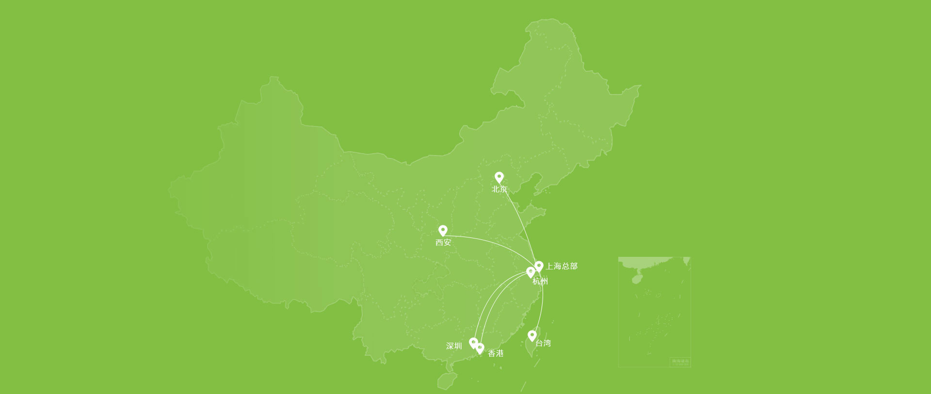
S2Cは今日の革新的なSoC/ASICデザインに向けたFPGAプロトタイピングの世界的リーダーです。2004年の設立以来、S2Cは多くのラピッドSoCプロトタイピング・ソリューションを提供しています。600以上の顧客に4,000以上のシステムの導入実績を誇っており、優秀なエンジニア・チームと顧客重視を主義とする営業チームは、ユーザのSoC開発におけるニーズを十分に把握しています。S2Cは販売拠点および代理店を米国、欧州、イスラエル、中国、香港、韓国、日本、台湾に設けています。


会社概要

会社名

S2Cジャパン株式会社

設立

2014.6.16

本社所在地

143-0052

東京都大田区蒲田 5-8-7

蒲田K-1ビル 2

電話番号: 03 6404 9090

ファックス: 03 6450 0805


役員

代表取締役      辻智之

取締役          中間俊雄


資本金

2,000万円

主要取引銀行

みずほ銀行 新横浜支店

業務内容

SoC/ASICプロトタイプシステムの開発・製造・販売

各種電子回路、論理設計、基板製造受託業務

主な事業

上海总部

北京

新竹

西安

香港

深圳

杭州

日文.jpg

上海

デンマーク

イギリス

イスラエル

マレーシア

シンガポール

日本

韓国

ニュージーランド

オーストラリア

米国

インド

世界中に600以上の顧客を有しています。

詳しくは下記から

国内
国际
コアベネフィット
f1_i11.png f1_i1.png
顧客との信頼関係
——
f1_i21.png f1_i2.png
カスタムの柔軟性
——
f1_i31.png f1_i3.png
高い付加価値
——
f1_ic41.png f1_ic4.png
イノベーション
——
f1_i51.png f1_i5.png
即応性
——
開発パス
mdm
2021
  • Released Prodigy Mulit-Debug Module Pro

LX1.jpg
2020
  • Release Prodigy S7 Virtex UltraScale+ Logic System

  • Release Prodigy Logic Matrix

2019
  • Release Stratix-10 10M Logic Systems
LS.jpg
2018
  • Release Virtex UltraScale Logic Systems
2017-1.jpg
2017
  • Release Arria-10 & Stratix-10 Logic Systems
2016
  •  Release the prototype verification system capable of achieving 1 billion gate designs
2015-1.jpg
2015
  • Release Virtex & Kintex UltraScale Logic Modules
2013
  • Provides the largest library of off-the-shelf interfaces and accessories for FPGA-prototyping
2012-1.jpg
2012
  • Release Virtex-7 & Kintex-7 Logic Modules
2010
  • Release Stratix-4 & Virtex-6 Logic Modules
2008-1.jpg
2008
  • Release Virtex-5 Logic Modules
PlayerPro.jpg
2007
  • Release Design automatic segmentation software
2006-1.jpg
2006
  • Release Virtex-4 Logic Modules
2005
  • Release Virtex-2 Pro IP Porters
2004
  • Base in Shanghai, establish R&D and technology support center
2003
  • S2C was founded in San Jose, Californiar
2021
2020
2019
2018
2017
2016
2015
2013
2012
2010
2008
2007
2006
2005
2004
2003
名誉
f1_t1.png
ISO 9001
2021 China
IC Design Awards
United States Patent
Patent No. US009032344B2
2012.jpg
United States Patent
Patent No. US008607174B2

試作検証プランを入手

どのタイプのチップを設計していますか?
設計に含まれるASICゲートの容量は?
500万~2000万
2,000万~5,000万
5000万~1億
1億~10億
10億以上
どのFPGAを使いたいですか?
ザイリンクス VU440
ザイリンクス KU115
ザイリンクス VU19P
ザイリンクス VU13P
ザイリンクス VU9P
インテル S10-10M
インテル S10-2800
わからない、専門家のアドバイスが必要
どのようなFPGA構成が必要ですか?
シングルFPGA
デュアルFPGA
4 つの FPGA
8つのFPGA
わからない、専門家のアドバイスが必要
どのような周辺機器インターフェースが必要ですか?
プロトタイプ検証プラットフォームはいくつ必要ですか?
以下のツールが必要ですか?
セグメンテーションツール
複数の FPGA デバッグ ツール
コモデリング ツール (FPGA と PC ホスト間で大量のデータをやり取りできます)
当社の製品をいつ使用する必要がありますか?
0~6ヶ月
6-12ヶ月
12ヶ月以上
わからない
その他
参加する
電話番号を入力していただければ、すぐに折り返しご連絡いたします
あなたの電話を入力してください
検証コード

This site uses cookies to collect information about your browsing activities in order to provide you with more relevant content and promotional materials, and help us understand your interests and enhance the site. By continuing to browse this site you agree to the use of cookies. Visit our cookie policy to learn more.