Ablaze Wireless was founded in 2008 with the goal of providing highly secured, cost effective solutions to the femtocell market. Over the course of the past few years, the company has achieved the impossible by delivering quality products with innovation while still staying lean. In 2009, Ablaze Wireless expanded its operation by setting up an office in Taipei, Taiwan to work closely with the supply chain and manufacturers to bring down the cost of femto access points.


Ablaze Wireless focuses on the femtocell market with the mission of providing highly secured, cost effective solutions to our customers. So we must always keep up with the challenges of innovation in this industry, speeding up product development cycles and reducing time to market. As Albaze's design size grows rapidly, prototyping our design on FPGA becomes very complex, which then requires splitting the design into multiple FPGAs and debugging such a complex FPGA system. Ablaze Wireless does not want to be involved with solving such problems as building and debugging a multiple FPGA board and wants to dedicate resource on the innovation of our technology.
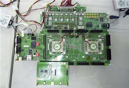
Ablaze Wireless originally discovered S2C from the Altera Website. After careful research, Ablaze Wireless felt that the S2C Sratix-4 820 platform provided the best combination of performance, features and cost advantages. Everything went well and we purchased two Dual Stratix-4 820 FPGA prototyping platforms and used the FPGA platforms for both hardware bring-up and hardware software co-development.
The fact that we could develop our production- quality software and verify it on our SoC prototype based on FPGAs, before making the final decision to tape-out provided us with tremendous advantage. The Dual Stratix-4 820 Platform enabled us to put more of our SoC design on the FPGA platform at a time than what we could before. Fast USB FPGA image download is a real time saver. And, Prodigy Player Pro Software also provided us with a greater level of control compared to our previous platform.
Prodigy™ Player Pro Software provided us with a greater level of control compared to the previous platform
The fast USB FPGA image downloading is a real time saver
The larger gate capacity enabled us to put more of our SoC logic onto the FPGA platform at a time, reducing the number of verification iterations needed
S2C's Dual Stratix-4 820 platform is well designed and feature rich, which reduced the overall design cycle time

S2C products improved the confidence level of Ablaze Wireless's SoC design robustness and accelerated the time-consuming iteration process between hardware and software prototyping cycles. For example, Ablaze Wireless could easily adjust the reference clock frequencies via Prodigy Player Pro Software, which allowed them to benchmark the clock frequencies vs. memory throughputs without having to compile multiple FPGA images. S2C FPGA platform was instrumental in helping to complete Ablaze Wireless's prototyping on time.
Compared with their prior experiences of using a competitor’s platform, Ablaze Wireless estimated that the S2C platform shortened their development cycle by 3~6 months, due to the larger capacity, improved stability, and the abundance of connectivity options. Ablaze Wireless look forward to using more advanced S2C verification software such as DPI and C-API to speed up our cycle-based simulations in the next project.


This site uses cookies to collect information about your browsing activities in order to provide you with more relevant content and promotional materials, and help us understand your interests and enhance the site. By continuing to browse this site you agree to the use of cookies. Visit our cookie policy to learn more.