Five Challenges to FPGA-Based Prototyping |
Ron Green, S2C Inc. 9/19/2014 01:05 PM EDT
The state of the art has progressed spectacularly since early forays into FPGA-based prototyping, but there are still challenges to be overcome.
What is FPGA prototyping, and why should I care? Not long after the introduction of FPGAs in the late 1980s, engineers seized upon these devices for building system prototypes of ASIC and SoC designs. Containing vast amounts of configurable logic, these versatile components were a natural choice for building and testing the latest designs. As designs grew in both size and complexity, FPGAs also grew to provide ever-increasing (equivalent) gate counts.
With earlier generations of FPGAs, it often took a large array of devices to fully accommodate a logic design. However, using today's devices with their mega-million gate counts, it may require only a handful of devices -- or even just one -- to implement a complete design.
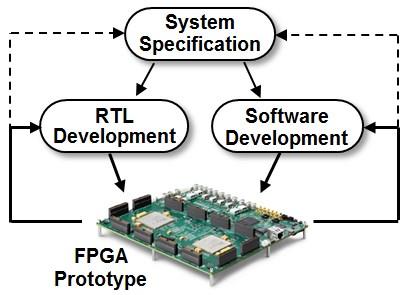
The utility of a working FPGA prototype is undisputed. It allows hardware designers to develop and test their systems, and it provides software developers early access to a fully functioning hardware platform.

There are a number of key advantages that FPGA-based prototypes provide. These may be summarized as follows.
Five challenges Despite the advantages provided by FPGA-based prototyping, there are some significant hurdles to overcome. The five challenges presented below surfaced early on, and they haven't changed much over the years.
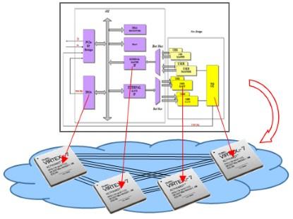
1. Design partitioning: Not many designs fit in a single FPGA; designs often must be partitioned across several devices. Initially, there were no tools to automate partitioning, so this task was tedious and error-prone. Worse still, designs that are split arbitrarily among several devices require a great deal of interconnect, which quickly surpasses the number of I/O pins available. Solving this problem requires a pin-multiplexing scheme.

2. Long bringup: Though engineering teams can design, build, and bring up a prototype, it can take a significant amount of effort. PCBs built to accommodate multiple FPGAs require numerous layers, and bringing up such a prototype typically requires verifying connectivity for more than 10,000 signals and pins. Mapping a design to FPGA prototype hardware can also be time-consuming and prone to error. When a design does not work in a prototype, it can be because of physical problems, design errors, or mapping issues. Without good techniques and the necessary tools, bringing up a prototype board can add months to your project schedule.
3. Difficult debug: It used to be that signals internal to an FPGA could not be probed unless they were brought out through the input/output (I/O). Fortunately, major FPGA vendors today have internal logic analyzers to address the visibility issue. However, many of these internal logic analyzers have several limitations, including support for only single FPGA debug, limited memory size using FPGA internal memory, and long place-and-route times to change probes.
4. Performance: After all this effort, the prototype may not perform as expected. Issues related to PCB physics -- such as signal routing, capacitive loading, and impedance matching -- will limit how fast the prototype can run. Considerations such as partition strategy, pin multiplexing, clock conversions, and FPGA timing constraints will also impact performance. Add to this the demands of high-speed transceiver interfaces -- such as PCIe, SATA, and 10G Ethernet -- that run in the GHz range. Without good design practices and reference designs, it is difficult to achieve the target performance in one pass.
5. Reusability: The ability to reuse a prototype (or even part of one) can save development time and lower implementation risk for future projects. But this is difficult to achieve with boards built for a specific project. As SoC designs grow in size, they may no longer fit in older FPGAs. If the interface to an external system is built directly on the prototyping board, it can't be reused for projects in which the interface is different.
Addressing the challenges With the advent of very large FPGAs, the problem of design partitioning diminishes to some degree. However, these devices also come with large pin-outs (e.g., some Xilinx Virtex-7 packages have nearly 2,000 pins), requiring boards with 18 signal layers (or more) coupled with multiple voltage planes. Large boards with a high number of interconnects still present many challenges. To handle the latest designs mapped to the latest devices, solutions like the following are required.
Due to these complexities -- and because development schedules don't allow time to develop a prototype from scratch -- commercial off-the-shelf prototyping and emulation systems have all but replaced internally developed solutions.
It's easy to see why this is the case. A robust off-the-shelf product provides guaranteed timing parameters, can be reused for multiple designs, and comes with dedicated technical support. The time spent on building a prototype from scratch is eliminated along with associated nonrecurring engineering (NRE) costs, which translates to realizing a working prototype faster with lower overall costs.
Selecting an FPGA-based prototyping system Ready-made prototyping solutions have become markedly more powerful in recent years, providing stable design environments and greater control through software and peripherals. There are a number of key parameters to consider if you're looking for an FPGA-based prototyping solution.
Capacity: Without enough gate-level capacity to accommodate your design, you can't build a prototype. Most systems need memory, too, so having sufficient memory available is critical.
Scalability: This is the ability to add capacity as needed, including gate-level and memory capacity. Scalability also deals with extensibility -- adding components such as processors and communication interfaces to grow the system functionality. Another dimension of scalability is system replication, the ability to quickly (and cost-effectively) produce copies of a given design for multiple deployments or intersystem testing.
Performance: The whole purpose of building an FPGA-based prototype is to achieve sufficient performance for the next level of tasks: hardware verification, software development and optimization, and system test. If your prototype can't deliver the performance, it will fail at its original purpose. Achieving performance requires the PCBs to be specially designed with careful interconnect and I/O design, including load balancing, clock performance, and the use of high-speed communication channels such as gigabit transceivers.
Compile/partition software: The ability to partition a design reliably across multiple FPGAs is critical to handling large designs. It's very important to have a software tool to make this task easy and reliable. The partitioning software must also optimize I/Os, clocks, and pin multiplexing to ensure maximum performance. Since the partitioning algorithms and hardware architecture are closely related, they yield the best results if they are considered together, so finding an integrated solution for this is preferred.
Debug tools: Debugging a design partitioned across multiple FPGAs is all but impossible without a tool that helps set up probes and makes signals easy to track based on their RTL-level names. Debugging should use FPGA I/O efficiently and maintain a useful debug trace depth.
Transaction-based interface: A recent DeepChip report stressed the importance of "transactors" -- interfaces that bridge the gap between abstraction levels. This could be a well-known bus protocol such as AXI or an industry-standard transaction protocol such as SCE-MI that communicates between a design mapped to an FPGA and a behavioral simulation. Transactors extend the functionality of the system, allowing it to be used for algorithm/architectural exploration, system integration with virtual prototypes, and exhaustive testing through software-generated corner tests. Where transactors are used, they must be efficient to avoid becoming bottlenecks to overall system performance.
Reliability: A reliable hardware platform is paramount. In order to ensure reliability, a system should have self-test capability and should include protection mechanisms to guard against problems such as overcurrent, overvoltage, and overtemperature.
Reusability: The ability to reuse your prototype platform enhances its usefulness, speeds the process of developing new prototypes, and reduces overall costs.
Remote management: Managing a prototype remotely makes it easier to deploy for multiple users and projects. As a result, prototype resources can be located anywhere -- in a centralized facility for easy maintenance, for example -- yet used by groups distributed around the world. The ability to download the FPGAs remotely makes it easy to reconfigure a system for any purpose.
Whither the state of the art? The state of the art has progressed spectacularly since early forays into FPGA-based prototyping. Commercial systems abound in both size and approach -- from huge emulation boxes costing millions of dollars to modest providers with small, low-end boards.
In your search for a solution, when comparing offerings from different vendors, I would urge you to take a look at the systems from S2C Inc., the company where I work. We offer a wide range of rapid prototyping solutions providing tremendous gate-level and memory capacity, all built upon the latest Xilinx and Altera FPGAs. You'll find a family of systems that are scalable, extensible, and reusable; that support advanced debug tools that work across multiple FPGAs; and that include transactors such as an AXI bus interface and a C-API to ease integration with other systems. Offering many advanced features, S2C's FPGA-based prototyping systems are extremely cost-effective. They are among the most advanced in the world, and they are built to handle the most ambitious design challenges.
-- Ron Green is the technical communications manager with S2C Inc. Prior to this, he was with Cadence Design Systems and Altos Design Automation. He has held various positions, including design engineer, AE, technical trainer, and technical writer. He appreciates clever designs, compelling materials, and the espressos at Mr. Toots Coffeehouse.


This site uses cookies to collect information about your browsing activities in order to provide you with more relevant content and promotional materials, and help us understand your interests and enhance the site. By continuing to browse this site you agree to the use of cookies. Visit our cookie policy to learn more.