WEBNAR: How ASIC/SoC Rapid Prototyping Solutions Can Help You! |
Daniel Nenni Published on 08-23-2019 at 10:00 am
If you are considering an FPGA prototype for an ASIC or SoC as part of your verification strategy, which more and more chip designers today are doing to enhance verification coverage of complex designs, please take advantage of this upcoming webinar:
How ASIC/SoC Prototyping Solutions Can Help You!
Or to get a quick quote from S2C click here.

S2C has been developing FPGA prototyping platforms since 2003, and, over the years, they have figured out what users want for a complete FPGA prototyping solution.
If you are new to FPGA prototyping, the S2C website provides a good overview of what to consider as you begin your project; your Application type, your Design Stage, and your Design Classification. If you are an experienced FPGA prototype user, and you know what you need, then you can skip the preliminaries and go straight to the Products and Services tabs. Here you will find a comprehensive display of the hardware and software products that S2C has available to support your FPGA prototyping project, along with custom FPGA prototyping and verification services.
S2C supports both Xilinx and Intel FPGAs, as well as different size FPGAs from each of these two leading FPGA providers. To further support a wide range of design complexity options, S2C offers Single, Dual, and Quad FPGA platforms. For Enterprise-class prototyping, S2C offers the Prodigy Cloud Cube, which supports up to eight Quad Logic Modules with a total of up to 32 FPGAs.
S2C prototyping platforms are available in two configurations; Logic Modules, and Logic Systems. Logic Modules take a “component” approach to the FPGA hardware with separate FPGA Module and Power Supply. Logic Systems are a newer integrated, modular configuration that includes up to four FPGA Modules, a Power Control Module, and the Power Supply, all in a single low-profile enclosure.
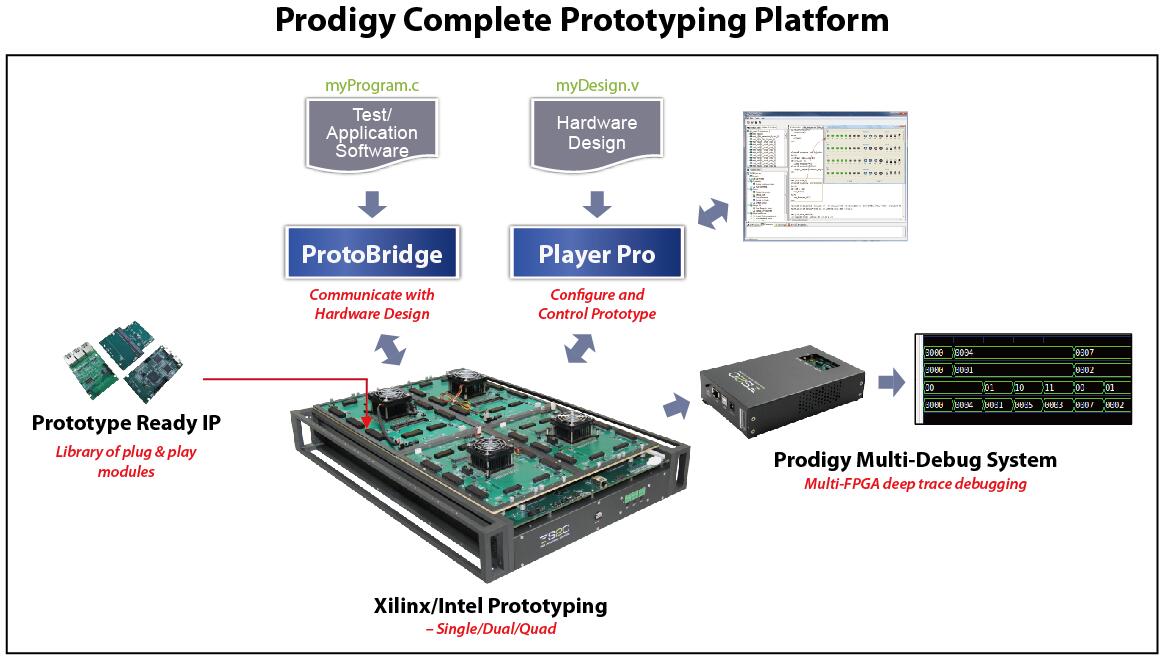
S2C’s “complete FPGA prototyping solution” includes additional hardware and software products that complement their FPGA Logic Modules and Logic Systems;
PlayerPro Runtime software is included with S2C’s FPGA hardware, and configures the FPGA prototype, provides for remote system management and facilitates debug set-up. PlayerPro Compile software is an optional integrated GUI environment and Tcl interface that enables users to compile and partition a design into multiple FPGAs, and generate the individual FPGA bit files. If a single FPGA is all you need, PlayerPro Runtime will provide everything you need to set-up, run, and debug your FPGA prototype.
ProtoBridge is an out-of-the-box hardware and software solution for applying large amounts of test data in the form of bus traffic, or communications traffic, or video images, etc. to the FPGA prototype from your host computer. ProtoBridge includes AXI master/slave and PCI bridge modules that are compiled and loaded into the FPGA with the prototype design, physical PCI cable hardware that supports up to 1GB/s transfers, PCI driver software, and a set of C-API function calls to drive AXI bus transactions from the host computer.
The Multi-Debug Module (“MDM”), supports very wide and very deep test data traces up to 32K signals per FPGA, in 8 groups of 4K probes per FPGA, without re-compile, and can store 8GB of waveform data without consuming user memory (MDM hardware includes memory), with a rich selection of trigger event conditions. MDM provides the unique ability to view waveforms from multiple FPGAs in a single viewing window.
Prototype Ready IP (a.k.a. “Daughter Cards”) rounds out S2C’s complete solutions for fast, reliable FPGA prototype project ramp-up. With more than 80 Daughter Cards, S2C offers a rich off-the-shelf library of I/O interfaces (USB, PCI, GPIO, etc.), Clock Modules, Multimedia Interfaces (MIPI, HDMI, etc.), Memory Modules, ARM and Zynq Interface Modules, and Cable Adapters. S2C’s Daughter Cards attach to the FPGA modules using high-quality, high pin-count connectors for quick, reliable, Tinkertoy-like assembly.
Then, if you have some unique FPGA prototyping requirement that is not met by S2C’s off-the-shelf products, they will also entertain discussions for joint development of custom Daughter Cards, FPGA Boards, and other FPGA prototyping services.
So, if you are considering FPGA prototyping for the first time, or you are looking to upgrade your FPGA prototyping capabilities for more complex designs please register for this webinar and find out everything you need for FPGA prototyping:
How ASIC/SoC Prototyping Solutions Can Help You!
Or to get a quick quote from S2C click here.


This site uses cookies to collect information about your browsing activities in order to provide you with more relevant content and promotional materials, and help us understand your interests and enhance the site. By continuing to browse this site you agree to the use of cookies. Visit our cookie policy to learn more.