

AI Chip Prototyping Plan |
|
Daniel Nenni Published on 07-03-2019 08:00 AM
I recently had the opportunity to sit down with a chip designer for an AI start-up to talk about using FPGA prototyping as part of a complex silicon verification strategy. Like countless other chip designers for whom simulation alone simply does not provide sufficient verification coverage, this AI start-up also believed that FPGA prototyping would be a critical part of a successful chip delivery plan. When millions of dollars are at stake for advanced silicon geometry masks, not to mention the potentially fatal consequences of a startup missing a market window, getting silicon right the first time is key to success. This AI chip designer was running into FPGA prototype platform capacity limitations … and running out of time.
Throughout our discussions I couldn’t help being reminded of the value of a well thought out FPGA prototyping Plan early in the chip development process to minimize nasty surprises late in the design cycle. Considerations like: what chip functionality needed to be prototyped and when, estimated FPGA gate capacities, what prototype performance would be needed, how the prototype would be tested, etc. In addition, FPGA prototypers should consider how could the FPGA prototype will be easily scaled from one phase of prototyping to the next.
We reviewed the AI chip designer’s FPGA prototyping “vision”, and what options were available to complete the FPGA-based verification, and then scale up for customer demonstration platforms and more comprehensive design verification. The conversation revealed that there were three phases envisioned for FPGA prototyping;
· Phase 1 – verification of a “minimum slice” of the AI chip including a few AI processor cores before tapeout
· Phase 2 – an FPGA platform for a “larger slice” of the AI chip including more AI processor cores for early customer demonstrations, preferably before tapeout to assure alignment with customer needs
· Phase 3 – at some later stage, an FPGA prototype of the whole AI chip, where the whole AI chip would require about one billion equivalent ASIC gates from the FPGA prototype! Yes, that’s billion with a “B”.
Phase 1 was the immediate concern for this AI project, and a solution was needed quickly to allow enough time for good AI chip test coverage before tapeout. With minimum resources, start-ups do not have the luxury of major late-stage corrections to any part of their verification strategy, so changing FPGAs to get more gate capacity would require some trade-offs; do less with the available FPGA platform, or change to a bigger FPGA and run the risk of impacting tapeout schedules. FPGA gate capacity scaling can be accomplished by changing to a larger FPGA, or by using multiple FPGAs with the inherent need to partition the design between the multiple FPGAs … each approach has its pluses and minuses when it comes to impacting project effort.
Phase 2 should be scalable from Phase 1, if the Phase 1 FPGA platform provides a smooth path to scale up gate capacity for Phase 2. If Phase 2 calls for multiple FPGAs, and the Phase 2 approach is a linear scale up from Phase 1, which is usually the case with AI chips composed of a large array of identical processors, the choices made for the Phase 1 platform can simplify the Phase 2 solution.
Phase 3, at a billion gates, requires a separate discussion, and traditional emulation is the easy answer. The challenges with emulation are cost and performance. This AI company has considered emulation but found it simply too expense for a start-up. The company thinks it has the technical expertise to build a billion-gate FPGA prototype but has the good sense to admit that such an undertaking would be monumental and not the primary focus of their business. And then there is emulation performance, which sacrifices performance for high design visibility. While an emulator can achieve performances of close to 1MHz, FPGA prototypes are capable of performances of tens of MHz.
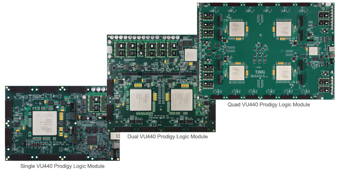
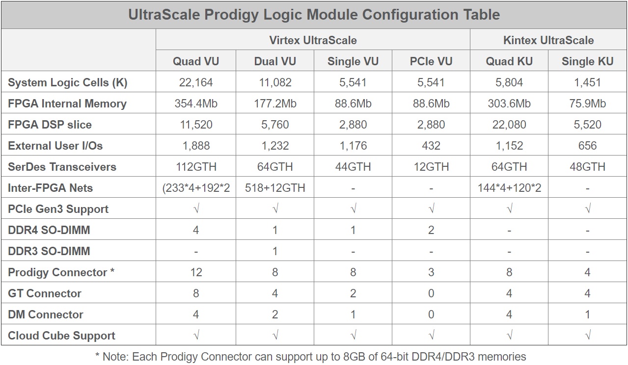
S2C’s Prodigy Family of FPGA prototyping solutions provide ample FPGA gate capacity options using either Intel FPGAs or Xilinx FPGAs … the user may choose their favorite brand of FPGA, a decision which is usually based on design tool preferences. The largest Xilinx FPGA is the VU440, which will support 30M to 40M effective logic gates, assuming a conservative gate utilization of 50% to 60%. Prodigy Logic Modules come with one (Single), two (Dual), or four (Quad) VU440 FPGAs, which translates conservatively to a range of available gate capacities from about 30M gates to over 100M gates.
The Prodigy Family also offers a high speed channel for the transfer of large amounts of transaction-level data between the FPGA prototype and a host computer (ProtoBridge), multi-FPGA debugging that allows deep off-chip trace storage (8GB), multi-FPGA trace viewing in a single window (MDM), and a rich family of ready-made daughter cards (80+) for quick assembly of a prototyping context.
S2C has been in the FPGA prototyping business for over 15 years, so their prototyping hardware is solid. S2C pricing for the VU440 Logic Modules starts at under $50K for a Single Logic Module and scales up to the Quad Logic Module. To get a quick S2C quote click here.


This site uses cookies to collect information about your browsing activities in order to provide you with more relevant content and promotional materials, and help us understand your interests and enhance the site. By continuing to browse this site you agree to the use of cookies. Visit our cookie policy to learn more.


-383.png)


