

FPGA-Based Prototyping: Big Design – Small Budget? |
 |
Mon-Ren Chene, S2C Inc. 11/19/2014 02:06 PM EST
Recent advancements in partitioning, debug, and scalability have made FPGA-based prototyping the ideal solution for even the largest ASIC/SoC designs.
A recent article, "Five Challenges to FPGA-Based Prototyping," explored some of the questions regarding FPGA-based prototyping and helped debunk the myths surrounding the issues of bring-up time, debug, performance, and reusability.
Over the next several articles, we'll look into the specifics of how FPGA-based prototyping can accelerate your design and verification.
There is a common misconception that FPGA-based prototyping is only suited to small designs and that the advantages of the technology diminish as designs grow. For verifying large designs, emulation is often the first technique that comes to mind. Now, emulation is fine for verifying large designs, but it comes at a cost. There is a penalty in both speed and price.
Emulation can be very slow at modeling your design, thereby impacting attempts at early software development. And emulation is expensive, putting it out of reach for companies on a budget. Every engineering manager is faced with considering time and cost tradeoffs to meet stringent time-to-market windows. To put these tradeoffs into perspective, let's first examine the advances in FPGA-based prototyping technology that help to close the gap between design size, speed, and cost.
FPGA technology advancements FPGA capacity has increased exponentially over the years. Today's largest V7 FPGAs from Xilinx based on a 28nm process have the capability to hold the equivalent of up to 20 million ASIC gates. By using an array of such FPGAs, we can leverage this further, with the potential to build a system that is close to half a billion ASIC gates. And the next generation of FPGAs, such as Virtex-UltraScale based on a 20nm process, holds even greater promise -- the prospect of building a practical and affordable system containing up to a billion gates.
FPGA-based prototyping can also run at much higher speeds than emulation. Internal FPGAs can run at hundreds of MHz, and I/Os can run at the multi-GHz range depending on the I/O standard. Even with very large FPGA prototyping systems, you can still expect anywhere from 5 to 20MHz system speed. This is an order of magnitude faster than emulation, which usually runs in the sub-MHz range.
To explore this idea of using FPGA prototyping for big designs further, let's look at the key technology considerations for adopting prototyping for these designs.
Partitioning Partitioning is key when prototyping a large design using FPGAs. In the past, with smaller FPGAs, partitioning required cutting through an IP block and distributing it across multiple devices. Today, most design blocks easily fit within one FPGA, so partitioning is primarily the process of grouping select IP blocks together onto a single device. Furthermore, the adoption of new FPGA I/O technology such as 1GHz LVDS enables the interconnection of more I/Os between FPGAs using a pin-multiplexing scheme.
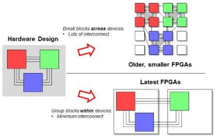
Partitioning software should also be considered. Along with other partitioning technology, the quality and usability of partitioning software such as Flexras and Mentor's Auspy have also significantly improved over the years. Similarly, the commercial partitioning tool from S2C has been used to partition a multi-core CPU design across 20 FPGAs.
Debug Partitioning and implementing the design in multiple FPGAs doesn't mean much unless you have the ability to debug the design effectively and efficiently. Many debug tools, including those provided by FPGA vendors, can only be used on a single FPGA. This is okay if you only have a single FPGA design or if you have the time to debug each FPGA on your system separately. But this can be both time-consuming and highly error-prone. In addition, most of these debug tools utilize the FPGAs' internal memories, which results in very limited trace depth. Debugging a multi-FPGA design works better if you can look at multiple FPGAs at the same time. This reduces both debug time and errors, while also using external memory for increased capacity.
S2C offers a unique multi-FPGA debug solution that uses an external FPGA to connect to multiple FPGAs at the same time via Gigabit Transceivers and stores the captured waveforms on 16GB of external DDR3 memory.
Due to its speed, FPGA-based prototyping is ideally suited for identifying and locating such bugs as critical corner cases, bugs related to subjective data, and bugs that require extremely long runs of actual system data. With larger designs, it is critical to adopt FPGA-based prototyping debug earlier in the process so as to help reduce late-stage ECOs.
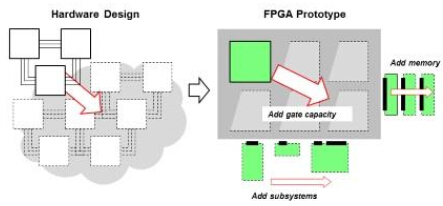
Scalability FPGA-based Prototyping can be used at various design stages such as algorithm/architectural exploration, IP development, and full SoC in-circuit testing. Having a scalable or modular FPGA-based prototyping system will maximize your investment so various design projects at different design stages can all share the same platform.
Having said all this, you need to perform due diligence when evaluating potential FPGA-based prototyping systems. There are some such systems that are too specific in their use model to achieve this level of scalability. For example, FPGA boards utilizing PCIe are hard to scale beyond four FPGAs. Interconnections, global clocks, system control of multiple boards, power, and mechanical considerations become un-manageable. Most of these solutions also require too many cables making expansion unwieldy.
The following points should be considered in order to avoid any pitfalls:
Budget tradeoffs As previously mentioned, engineering managers are consumed with overall budget tradeoffs. It is of utmost importance to strike the optimal balance between cost, resources, and time in order to achieve the necessary goals. Now, with the advances in FPGA-based prototyping technology to handle large designs, managers should take a second look at how to apply resources to their design.
Emulation, although effective, is expensive. Emulation also has debug limitations that FPGA-based prototyping can tackle much faster, thereby making a strong case for applying FPGA-based prototyping sooner so as to save time later in the flow. If a manager can apply a less expensive FPGA-based prototyping methodology sooner in the verification process, this could save hundreds of thousands of development dollars.
The cost and speed of FPGA-based prototyping has always been a good fit for smaller designs. The solution provided by S2C is a unique example of a system addressing these needs. Our offering allows one, two, and four FPGAs on a single prototyping board that can then be used in conjunction with other boards (using stacking/cabling or located in a chassis) to provide a system with up to 32 FPGAs. Using boards carrying a single FPGA module to form a big system offers maximum flexibility; using boards carrying four FPGA modules achieves minimum cabling.
The end result is that recent advancements in partitioning, debug, and scalability have made FPGA-based prototyping the ideal solution for even the largest ASIC/SoC designs.
— Mon-Ren Chene is currently the Chairman and Chief Technology Officer for S2C. He has more than 30 years of engineering and management experience in EDA and FPGA software/application development. He co-founded Osprey Design Systems that later merged with Aptix, where he served as Software Architect and VP of Software Development. Chene also held engineering and management positions at Quickturn Design Systems, Xilinx, Cadence Design Systems, Silvar-Lisco Design Systems, and NCA. He holds five US Patents and three pending patents. He is a graduate of Stanford University with an MS in operations research.
— Max Maxfield, Editor of All Things Fun & Interesting


This site uses cookies to collect information about your browsing activities in order to provide you with more relevant content and promotional materials, and help us understand your interests and enhance the site. By continuing to browse this site you agree to the use of cookies. Visit our cookie policy to learn more.


-383.png)


