

S2C's FPGA-Based SoC Prototyping System Supports PCIe 3.0 Cores |
 |
Max Maxfield 8/18/2014 05:55 PM EDT
When it comes to developing new ASIC, ASSP, and SoC designs, FPGA-based prototyping systems offer a number of advantages over other prototyping solutions. These advantages include extremely high "hardware-level" speed at relatively low cost.
S2C offers a variety of FPGAS-based prototyping platforms, including the V7 TAI Logic Module, which boasts four Xilinx Vitex-7 2000T FPGAs that can accommodate the equivalent of 80 million ASIC gates.
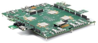
The V7 TAI Logic Module has four onboard DDR3 SO-DIMM sockets that can support up to 32 GB of DDR3 memory. The QuadE version offers 48 channels of high-speed gigabit transceivers that can run up to 10 Gbit/s and support designs using high-speed interfaces such as PCIe, SATA, and XAUI.
S2C has announced that Northwest Logic's PCI Express (PCIe) 3.0 solution -- including the Expresso 3.0 Core (PCI Express 3.0 Controller Core) and family of DMA Cores -- has been validated and certified for use with S2C's ASIC prototyping platforms. This validation and certification was performed with eight lanes running at 8 Gbit/s SerDes rates.
With some FPGA-based hardware prototypes, third-party interface subsystems like PCIe are delivered only as RTL, which has to be synthesized along with the rest of the design and ends up consuming a large proportion of the prototyping platform's FPGA resources. To get around this problem, S2C has developed a Prototype Ready suite of IP cores.
In the case of Prototype Ready IP cores, in addition to the RTL that will form part of the final ASIC/SoC design, an accessory module containing a hardware implementation of the core can be plugged on top of the TAI Logic Module as a daughter card. (Multiple accessory modules can be plugged into a TAI Logic Module.) This is the way Northwest Logic's PCIe 3.0 solution is presented -- as a Prototype Ready IP core module for use with the TAI Logic Module.
Please visit the S2C or Northwest Logic websites for more information.
— Max Maxfield, Editor of All Things Fun & Interesting 


This site uses cookies to collect information about your browsing activities in order to provide you with more relevant content and promotional materials, and help us understand your interests and enhance the site. By continuing to browse this site you agree to the use of cookies. Visit our cookie policy to learn more.


-383.png)


