
The shift from local applications to cloud computing services is ever present not only with intercompany communications but also among consumers-to-consumer, business-to-consumer, and business-to-business applications. As data becomes increasingly shared among users and the amount of data consumed skyrockets, the need for cloud-based data centers is imperative.
The massive amount of data must be delivered at lightening speed and always available. Of equal importance is that as communication bandwidth increases so does the amount of data and physical size of each piece of data. To handle the high performance delivery of this ever-growing amount of information, systems such as Supercomputing Centers and Cloud-based Content Delivery Networks (CDNs) have emerged. The architectural design of these systems is robust in both size and complexity utilizing vast arrays of buses, protocols, hybrid storage systems (HSS), and intricate software. The insatiable need by users for data and the complexities of these delivery systems makes it necessary for design engineers to employ the most efficient and effective design and verification solutions .

FPGA prototyping systems are the ideal solution for the design and verification of complex supercomputing and content delivery networks. Beyond the advances in partitioning and multi-FPGA debug that scale to meet any size design, FPGA-based prototyping allows designers to develop and test their systems well ahead of silicon providing software developers much earlier access to fully functioning hardware. The vast data centers are architected to perform a huge number of DSP algorithms and therefore the prototyping hardware must keep pace. S2C’s series of Prodigy Kintex UltraScale Logic Modules are ideal for the DSP-intensive applications that supercomputing and cloud-computing designs require. Scalability is a fundamental requirement for data intensive applications.
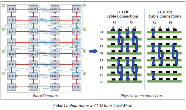
The use of S2C’s Prodigy Cloud Cube™, an enterprise-class, FPGA-based prototyping system that supports up to 32 FPGAs, using a combination of Prodigy Logic Modules, allows prototyping to scale with the size of the design. With the use of a MESH, multiple Logic Modules can be connected with a minimal number of cables to manage. The diagram below demonstrates how within a Cloud Cube a 4 x 8 MESH can map to 32 FPGAs with as little as 20 cables. Other solutions would need at least 156 cables to achieve the same architecture.
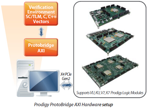
Particularly important to the development of these data storage and communication facilities is the ability to use transaction-level interfaces to bridge the abstraction level between behavioral models and live hardware providing a way to communicate between software running on a host and an FPGA-based prototyping platform that often includes memories, processors, and high-speed interfaces. S2C’s unique patent-pending Prodigy ProtoBridge™ System is a solution that allows for just this type of high-speed communication. ProtoBridge supplies a transactor interface between a software program and the world of AXI-compliant hardware. There are two key parts to this: an AXI-to-PCIe bridge that connects to a host computer, and a C-API that communicates to the design through the bridge. The software-to-AXI transactor offers new flexibility to designers building ARM-based systems. And coupling this to a PCIe interface supporting transfer speeds up to 500 Mbytes/sec, provides a perfect development platform for data-intensive applications.
A system like this allows designers to maximize the benefits of FPGA-based prototypes much earlier in the design project for algorithm validation, IP design, simulation acceleration and corner case testing. A prototype combined with a transactor interface makes a range of interesting applications possible throughout the design flow.
Solutions that Make the Grade
In addition to the important roles that our Prodigy KU Logic Modules, Cloud Cube and ProtoBridge System play in the world of supercomputing and cloud computing, S2C’s entire Prodigy Complete Prototyping Platform provides solutions for every aspect of your design flow. We provide the most comprehensive array of prototyping logic modules in addition to our KU offerings to fit your design size as well as the largest library of pre-tested prototyping IP and reference design flows to speed up and simplify your prototyping process. The Prodigy Player Pro Software helps to configure the prototype and provides remote system monitoring and control. The compile functionality within Player Pro offers advanced partitioning and the soon-to-be-released Prodigy Multi-Debug System will relieve the arduous and error-prone task of debugging each FPGA manually. Another solution on the near horizon is our Neuro™ software that manages parallel/remote software development among distributed hardware and design teams. S2C’s suite of Prodigy FPGA-based prototyping solutions is the most comprehensive on the market to help you realize the genius of your next design.


This site uses cookies to collect information about your browsing activities in order to provide you with more relevant content and promotional materials, and help us understand your interests and enhance the site. By continuing to browse this site you agree to the use of cookies. Visit our cookie policy to learn more.


-383.png)


