

Transactors -- Expanding the Role of FPGA-Based Prototypes |
 |
Ron Green, S2C 2/27/2015 05:30 PM EST
FPGA-based prototypes offer unbeatable flexibility, capacity, and speed. Extending their functionality through the use of a transactor interface opens up tremendous possibilities to designers.
Continuing the discussions we began by considering the Five Challenges to FPGA-Based Prototyping, we'll now take a look at some recent functionality this is now available with the most sophisticated prototyping platforms.
Power to spare It wasn't all that long ago that FPGA-based prototypes were the sole province of hardware designers and lab technicians. Viewed as finicky boards covered with rows of devices and bristling with cables, they were relegated to back rooms where engineers would endlessly tinker with them in a desperate effort to bring up designs of limited size and complexity.
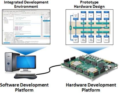
No more. Today's FPGA prototypes represent muscular platforms for developing ultra-large systems running at blistering speeds. With this kind of power, these systems are used for a wide range of tasks, including design integration, system verification, and software development (see also Big Design -- Small Budget?).
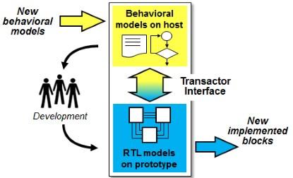
This solution is well-suited to designs fully rendered in RTL that can be mapped to an FPGA. But what about cases where portions of the design are still only available as behavioral models in descriptions such as C++ or SystemC?
FPGA-based prototypes to the rescue... again The latest systems now provide transaction-level interfaces -- often referred to as "transactors" -- that bridge the abstraction level between behavioral models and live hardware. Transactors offer a way to communicate between software running on a host machine and an FPGA-based prototyping platform that often includes memories, processors, and high-speed interfaces.
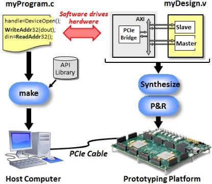
One example of this is the ProtoBridge system from S2C, which supplies a transactor interface between a software program and the world of AXI-compliant hardware. There are two key parts to this: an AXI-to-PCIe bridge that connects to a host computer, and a C-API that communicates to the design through the bridge. The software-to-AXI transactor offers new flexibility to designers building ARM-based systems. Also, coupling this to a PCIe interface supporting transfer speeds up to 500 megabytes/second provides a perfect development platform for data-intensive applications.
A Cornucopia of Applications A system like this allows designers to maximize the benefits of FPGA-based prototypes much earlier in the design project for algorithm validation, IP design, simulation acceleration, and corner case testing. A prototype combined with a transactor interface makes a range of interesting applications possible throughout the design flow:
The great facilitator The addition of a transactor interface to an FPGA-based prototype facilitates development of new systems in interesting ways. As behavioral models are introduced, architectures become refined and block functionality determined. These blocks are eventually defined and implemented as part of the new system. But blocks that are defined and rendered in RTL become IP for the next generation of systems, allowing the cycle of development to repeat. In this way, the FPGA prototyping platform becomes a great facilitator -- the engine of system advancement.
This combination is too powerful to ignore. FPGA-based prototypes offer unbeatable flexibility, capacity, and speed. Extending their functionality through the use of a transactor interface opens up tremendous possibilities to designers. These are tools and techniques no team should be without.
-- Ron Green is the technical communications manager with S2C Inc. His experience includes design and verification, IC layout, analog tools, cell characterization, emulation, and FPGA-based prototyping. A Silicon Valley veteran, Ron has held positions in engineering, applications, program management, and technical marketing. He appreciates clever designs, compelling materials, and the espressos at Mr. Toots Coffeehouse.


This site uses cookies to collect information about your browsing activities in order to provide you with more relevant content and promotional materials, and help us understand your interests and enhance the site. By continuing to browse this site you agree to the use of cookies. Visit our cookie policy to learn more.


-383.png)


