FPGA Prototyping of System-on-Chip (SoC) Designs | EE Times
Apr 08, 2015

FPGA Prototyping of System-on-Chip (SoC) Designs

The need for a complete prototyping platform for any design size at any design stage with enterprise-wide access, anytime, anywhere.


Mon-Ren Chene, S2C  4/8/2015 06:30 AM EDT

Today's off-the-shelf FPGA prototyping systems have established their value in every stage of the system-on-chip (SoC) design flow. Moving beyond traditional applications such as in-circuit testing and early software development, this technology has expanded to encompass functional design and verification (see also Transactors -- Expanding the Role of FPGA Prototypes).

FPGA-based prototypes work with electronic system level (ESL) design environments to refine, validate, and implement the chip's architecture, and with simulation tools to achieve an order of magnitude (or more) increase in verification speed.

There are several drivers of this technology: the need to quickly construct high-performance prototypes; the demands of growing design size and complexity (see also FPGA-Based Prototyping: Big Design – Small Budget?); and the need to utilize prototypes as an enterprise-wide resource. Globalization has replaced localized design teams with teams that are geographically-distributed. Consequently, FPGA prototyping solutions must now provide network access and remote management capabilities coupled with the ability to expand resources such as memory or add-on components. This allows realizing multiple hardware and software implementations for numerous, geographically-dispersed teams.

The FPGA prototyping system must offer enterprise-wide accessibility -- a complete prototyping platform is one that operates at any functional design stage, with any design size, and across multiple geographical locations. All of these capabilities must be available on-demand and be remotely-accessible at all times. Such an approach significantly increases engineering productivity and reduces the end-product's time to market, while increasing its return on investment (ROI), as well as increasing the lifetime ROI of the FPGA prototyping platform itself.

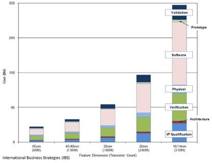
Growing SoC design challenges SoC size and complexity are increasing at an exponential rate. According to a keynote presentation by Gary Smith at the International Technology Roadmap for Semiconductors Conference in 2013, potentially available SoC gate counts will quadruple from 420 million in 2014 to 1.68 billion in 2020. International Business Strategies (IBS) reported that software development and hardware verification are the two leading factors in total SoC design cost (see Figure 1).

Figure 1. Software development and hardware verification are the predominant factors in SoC design cost (source: IBS). (Click here to see a larger image.)

These software- and complexity-driven cost and effort increases are accompanied by an elevated risk of late delivery, and even the possibility of outright failure. Cost and risk are generally mitigated by the extensive use and reuse of intellectual property (IP) -- both silicon and software -- but the complete silicon/software design must nonetheless be prototyped and tested as a whole.

FPGA-based prototyping solutions: Addressing today's needs For an FPGA prototype to meet the requirements of this "whole design", it must address the following criteria:

  • User access
  • Compile/partition efficiency
  • System interface capability
  • Scalability
  • Extensibility
  • Reusability
  • Analysis and debug capability
  • Application throughout the functional design flow

Utility of current FPGA-based prototyping systems

The key criteria for evaluating the utility of an FPGA-based prototyping system are as follows:

  1. Access to FPGA prototyping systems must not be constrained by the use of localized systems that require local management and control. Limited access can present a significant hindrance to modern SoC design teams -- especially software development teams -- which are often globally distributed.   
  2. The compile and build environment must incorporate important features such as the ability to partition a design automatically and/or with user guidance; automatic pin-multiplexing insertion and clock analysis. Also important are a convenient user interface to FPGA-specific place-and-route (P&R) tools allowing for quick flow turnaround for changes and ECOs.   
  3. Performance, which is the key reason teams develop FPGA-based prototypes. FPGA-based prototypes can be expected to realize system speeds in the tens of megahertz -- some have been known to run at 100MHz and more. High-speed FPGA prototypes enable early software development.   
  4. High-speed interfaces and add-ons, such as PCIe, USB, 10GE, ARM Debugger, and DDR memory are important for building a complete development platform. Transaction-level interfaces such as a CAPI and AXI bus protocol support greatly expand the utility of the system.   
  5. The ability to scale and extend the system is also an important consideration. This involves adding gate-capacity and memory, as well as processors and communication interfaces to grow the system's functionality.   
  6. Reusability is inherent in off-the-shelf FPGA prototyping systems. A system's reusability in subsequent designs is determined by the quantity and diversity of its resources -- gates, memory, and processing power. These resources must grow to remain up to date with changing functionality requirements.   
  7. Analysis and debug must not be limited to one FPGA at a time, which makes whole-system debug slow and tedious. Signal probing should work easily with designs partitioned across multiple FPGAs; a deep debug trace capability must be provided with probing schemes that maximize the use of FPGA pin I/O.   
  8. Support for a mixed-level prototype. Often during development, not all blocks are available in RTL. A complete prototyping system should support behavioral blocks running on a host computer to interface and communicate with RTL blocks mapped to the FPGAs.

The complete solution

Given the attributes and shortcomings of existing FPGA-based prototyping systems, what should be the attributes of the next generations of systems? As noted, the coming generations of off-the-shelf FPGA prototyping solutions must offer greater choice and flexibility in the deployment of resources. Consequently, the coming generations must take a "complete prototyping platform" approach as follows:

  1. Provide sufficient performance to operate as software development platforms. This requires PCBs with superior signal characteristics, clocking strategies, and connector structures.   
  2. Provide capacity, scalability, extensibility, and reusability. Modern FPGA-based prototypes can support designs from 20M to 500M gates. Add-on DDR2/3 modules can quickly create systems with multi-gigabyte memories. Peripherals and processors available on daughter cards make it easy to add various IP functionality.   
  3. Increase scalability, extensibility and reusability by enabling the deployment of an ever-increasing range of IP -- both silicon and software -- and pre-designed board-level subsystems. This requires the availability of copious IP and board-level reference design options.   
  4. Support the latest high-speed interfaces such as PCIe, HDMI, and 10Gig Ethernet.   
  5. Include an easy compile and build environment to accelerate the process of prototype bring up and ease the processing of design ECOs. Automatic partitioning tools should accept user input that can result in faster-running prototypes.   
  6. Offer global remote access to centralized prototyping resources, enabling access by multiple, geographically-distributed teams. This can be achieved by cloud-based control and storage.   
  7. Support behavioral/transaction-level interface and standard bus protocols such as AXI to ease system integration and provide a platform for software development.   
  8. Perform analysis and debug of the whole SoC design at full system speed with a focus on "deep" hard-to-find bugs. Simultaneously, it must achieve at least an order of magnitude increase in signal and cycle observability without consuming FPGA resources such as gates, memory, and I/O connectivity. This requires the implementation of structures that offer "pervasive observability" of design functionality. Fast probe-swapping is essential.   
  9. Continue to team with functional design and verification tools to perform tasks at every stage of the functional design flow, such as cross-leveraging the strengths of FPGA prototyping and simulation. This requires tight, well-integrated bridges between the diverse design environments.

Conclusion A modern FPGA-based prototyping system must meet a number of demanding criteria to help designers realize their latest system-on-chip designs. An extensible, scalable system must offer a variety of both hardware and software interfaces. High-performance and extensive debug capabilities are critical requirements. The ability to function as an enterprise-wide resource, with the easy access and configurability of a cloud service, multiplies the value of such a system. Meeting these criteria and combining features in a rich set of functionality qualifies a system as being a truly complete prototyping platform.

Mon-Ren Chene is currently the Chairman and Chief Technology Officer for S2C. He has over thirty years of engineering and management experience in EDA and FPGA software/application development. He co-founded Osprey Design Systems, which later merged with Aptix, where he served as Software Architect and VP of Software Development. Chene also held engineering and management positions at Quickturn Design Systems, Xilinx, Cadence Design Systems, Silvar-Lisco Design Systems, and NCA. He holds five US Patents and three pending patents. Chene is a graduate of Stanford University with an MS in Operations Research.

試作検証プランを入手

どのタイプのチップを設計していますか?
設計に含まれるASICゲートの容量は?
500万~2000万
2,000万~5,000万
5000万~1億
1億~10億
10億以上
どのFPGAを使いたいですか?
ザイリンクス VU440
ザイリンクス KU115
ザイリンクス VU19P
ザイリンクス VU13P
ザイリンクス VU9P
インテル S10-10M
インテル S10-2800
わからない、専門家のアドバイスが必要
どのようなFPGA構成が必要ですか?
シングルFPGA
デュアルFPGA
4 つの FPGA
8つのFPGA
わからない、専門家のアドバイスが必要
どのような周辺機器インターフェースが必要ですか?
プロトタイプ検証プラットフォームはいくつ必要ですか?
以下のツールが必要ですか?
セグメンテーションツール
複数の FPGA デバッグ ツール
コモデリング ツール (FPGA と PC ホスト間で大量のデータをやり取りできます)
当社の製品をいつ使用する必要がありますか?
0~6ヶ月
6-12ヶ月
12ヶ月以上
わからない
その他
参加する
電話番号を入力していただければ、すぐに折り返しご連絡いたします
あなたの電話を入力してください
検証コード

This site uses cookies to collect information about your browsing activities in order to provide you with more relevant content and promotional materials, and help us understand your interests and enhance the site. By continuing to browse this site you agree to the use of cookies. Visit our cookie policy to learn more.